Text
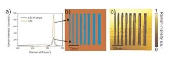
Within the European project Horizon 2020 - NextBase, we developed several characterization methods suitable for extremely thin layers (with a thickness below 20 nm). One of these methods utilizes the absorption of the Raman scattering signal of crystalline silicon by a thin layer of amorphous silicon deposited on this substrate. This non-contact method allows us to precisely determine the thin film thicknesses with a significant surface roughness. The method has been identified as a fundamental result of the EU project, therefore, we continue its development.
Cooperating institutions:
- PV-Center, Centre Suisse d’Électronique et de Microtechnique, Rue Jaquet-Droz 1, CH-2002 Neuchâtel, Switzerland (Bertrand Paviet-Salomon, Jonas Geissbühler, Matthieu Despeisse & Christophe Ballif)
- École Polytechnique Fédérale de Lausanne (EPFL), Institute of microengineering (IMT), Photovoltaics and Thin Film Electronics Laboratory, Rue de la Maladière 71b, CH-2000 Neuchâtel, Switzerland (Andrea Tomasi & Christophe Ballif)
- King Abdullah University of Science and Technology (KAUST), KAUST Solar Center (KSC), Thuwal, 23955-6900, Saudi Arabia (Stefaan De Wolf)
