RNDr. Martin Ledinský, Ph.D.
Employee function
Head of Working Group
Telephone
+420 220 318 467
E-mail
ledinsky [at] fzu.cz
Locality
Cukrovarnická
Room
C 211/7
Summary
Group activity
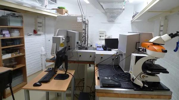
The group of Thin Films for Photovoltaic Applications is oriented towards depositions and nano-scale characterization of thin semiconducting films or selective contact used for photovoltaic purposes. Our aim is to probe alternative promising concepts and at the same time study the state of art materials and its properties with high spatial resolution.
In the last years, the main attention of this group was focused on four topics:
- Thin silicon based films used for passivation and as selective contact layers in heterojunction solar cells, in a frame of EU Horizont 2020 project NextBase
- Shallow doping (<10 nm) of the silicon surface by laser ablation or Schottky barrier on self-assembled carborane molecule monolayers.
- Halide perovskites for photovoltaic applications

