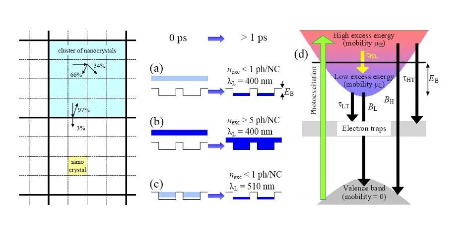
Ultrafast electron dynamics and short-range electron transport in CdS nanocrystals prepared by chemical-bath deposition were investigated in terahertz regime [Z. Mics et al., Phys. Rev. B 83, 155326 (2011)]. Initially high mobility of photogenerated electrons exhibits a decrease within 1 picosecond due to the relaxation of their excess energy. Role of nanocrystal surfaces and nanocrystalline aggregates in electron transport was elucidated.
Despite the fast development of optoelectronic applications of nanocrystalline materials, very little is known about interplay between charge transport and carrier confinement. The absence of a long-range crystal order fundamentally complicates the transport properties. In this work we used time-resolved terahertz spectroscopy to probe nanoscopic transport in nanocrystalline films of cadmium sulfide (CdS) prepared by chemical bath deposition. The sub-picosecond time resolution of the experiment allowed us to resolve the initial stages of the electron transport. The major conclusions are:
- Two length scales (nanocrystals and their clusters) control electron localization at the nanoscale. While interfaces between nanocrystals are highly permeable for electron transport, the interfaces between the clusters efficiently block the motion due to the existence of air voids.
- The efficiency of short-range transport is controlled by energy barriers due to electrostatic interaction between electrons and captured holes. The excess energy of electrons then plays the essential role in the conductive coupling between adjacent nanocrystals. (i) Relaxation of electrons with high excess energy leads to a decrease of their mobility on a subpicosecond time scale. (ii) Filling of conduction-band states by increasing the optical excitation fluence allows us to maintain a high level of conductive coupling even at later times.
