Core facilities of Laboratory of diamond thin films and carbon nanostructures consist of two unique microwave deposition systems Aixtron P6 and Roth & Rau AK 400. Both deposition systems represent a microwave plasma assisted chemical vapor deposition. At present time, the system Aixtron P6 is routinely used for growth of nanocrystalline diamond thin films (NCD) (Fig. 1).
Fig. 1: Left side - deposition system Aixtron P6 with ellipsoidal resonator cavity (installed in year 2002). Right side - large area deposition system AK 400 in configuration with linear antenna (installed at end of year 2008) – presently the unique system in Czech Republic which is industrially fully compatible for scaling are up to 1x1 m2.
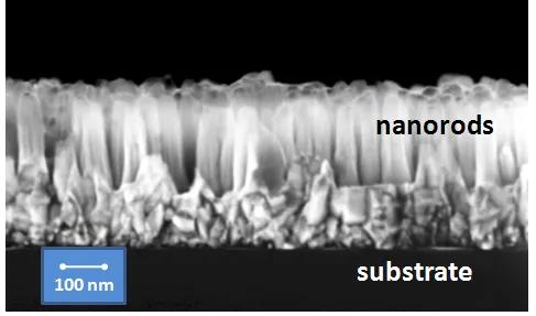
The typical size of film grains is 20-200 nm and the film thickness is 0,1 – 1 μm. Our NCD films exhibit excellent optical properties which very close to single crystalline diamond. Electronic quality of films is good enough for a fabrication of various demonstrators like FET transistors or gas sensors. In addition, a specific atomic termination of diamond films, i.e. oxygen or hydrogen, force the growth of osteoblas cells in predefined patterns. A significant progress in fabrication of diamond nano-rods and/or nanostructures has been achieved by using either top-down or buttom up strategy (Fig. 2). The long term visions focus on implementation of NCD films for interdisciplinary use in bio-nano-technologies with aim to better understand interaction of diamond surface with biomolecules, i.e. the interface organic and inorganic world. The basic fields, which are studied with supports and highly valuable expertise of cooperating groups mainly from the Instittue, can be summarized as follow:
- large area deposition of NCD films and other carbon forms (multi-wall carbon nanotubes, diamond nano-rods)
- optimizing of technological steps (deposition, plasmatic etching lithography, etc.)
- optically stimulated immobilization of (bio) molecules to diamond surface
- investigation of diamond surface interaction with atoms and molecules ( (DNA, proteins)
- fabrication of diamond base sensors and other demonstrators.
Fig. 2: Tilted (45o) SEM image of diamond nanorods (left) and cross-section view on diamond nanorods grown on Si substrate. Diamond nanorods were fabricated by reactive ion etching in O2/CF4 plasma and as masking material were used Ni nanoparticles.


